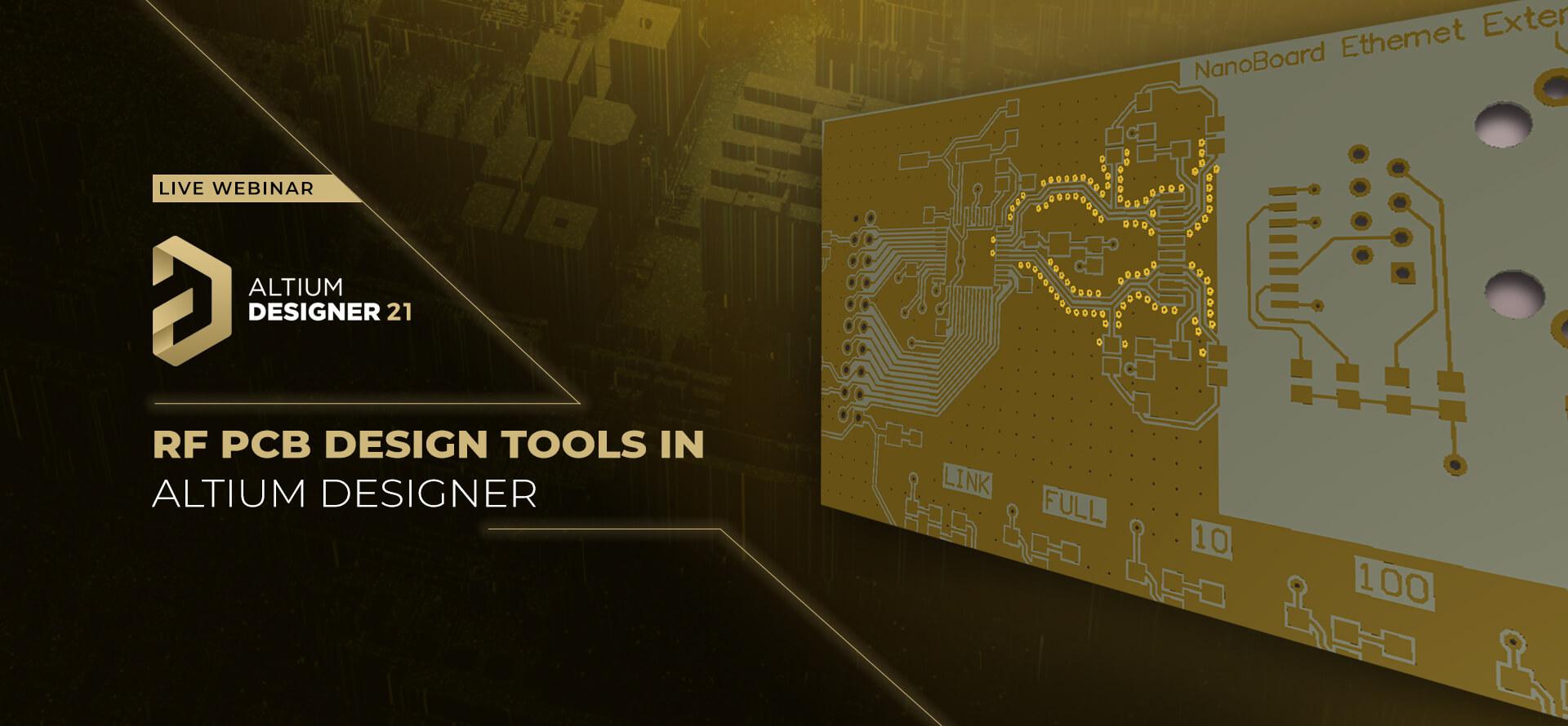
Live Webinar: RF PCB Design Tools in Altium Designer
RF stands for “Radio Frequency” There is a significant difference between standard PCB design and RF PCB Design. There are a lot of guidelines to develop the RF PCB design like proper coplanar impedance should be followed, suitable Material selection, Cross talk & EMI issues should be reduced, RF tracks isolation, Antenna design, RF Simulation, etc…
To implement these RF design guidelines what are the Tools and options we have in Altium Designer would you like to know?
Date : March 10, 2021
Time : 02:00 PM – 03:00 PM
Hosted by : Manimaran M,
Senior Field Application Engineer
Join this live webinar covering the following agenda:
- RF PCB Design Overview
- Some Basic RF PCB Design Guidelines
- Tools & Options For RF PCB Design in Altium Designer
- Demonstration
- Q&A